|
        

|
Atomic scale surface science
Scanning Tunneling Microscopy STM permits to study surfaces obtaining images in direct space with a resolution ranging from the nano to the atomic and sub-atomic scale (see STM photo gallery). At present the lab research is focused to the in situ study of surfaces and supported clusters produced by PLD (see figures on the right) and to the development of Scanning Tunneling Spectroscopy STS and sptin polarized STM (SP-STM) techniques to study electronic and magnetic properties of surfaces and isolated clusters with very high spatial resolution. Recently in collaboration with the SUSPENX group (prof. L. Braicovich, prof. F. Ciccacci) at Politecnico di Milano we developed bulk antiferromagnetic (cromium) tips for SP-STM. These tips allow to image Cr(001) surface with spin contrast.
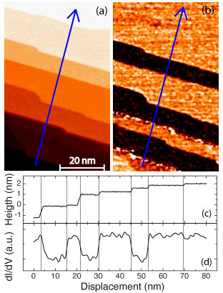
SP-STM images (topography and diffrential conductance) of
Cr(001) surface with a bulk Cr antiferromgnatic tip
Selected publications :
- C.S. Casari , S. Foglio, F. Siviero, A. Li Bassi, M. Passoni, C.E. Bottani
Direct observation of the basic mechanisms of Pd island nucleation on Au(111)
Physical Review B 79, 195402 (2009)
- M. Passoni, F. Donati, A. Li Bassi, C.S. Casari, C.E. Bottani
Recovery of local density of states using scanning tunneling spectroscopy
Physical Review B 79 , 045404 (2009)
- A. Li Bassi, C.S. Casari , D. Cattaneo, F. Donati, S. Foglio, M. Passoni, C.E. Bottani, P. Biagioni, A. Brambilla, M. Finazzi, F. Ciccacci, L. Duò
Bulk Cr tips for STM and Spin-Polarized STM
Applied Physics Letters 91 , 173120 (2007)
Selected for the Virtual Journal of Nanoscale Science & Technology (November 5, 2007)
- D.F. Leigh, C. Norenberg, D. Cattaneo, J.H.G. Owen, K. Porfyrakis, A. Li Bassi, A. Ardavan, G.A.D. Briggs
Self-assembly of trimetallic nitride template fullerenes on surfaces studied by STM
Surface Science 601 2750–2755 (2007)
<< back
|
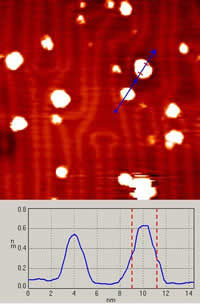
40x40 nm STM image of W clusters on Au(111)
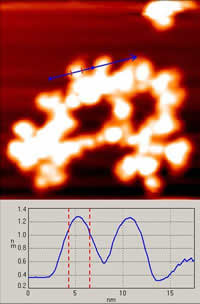
40x40 nm STM image of W clusters on HOPG
|